Contents
- Introduction
- Transistors
- Logic gates
- Multiplexors
- Combinational logic
- Sequential logic
- Clocking
- Conclusion
Introduction
Digital logic is concerned about how to route electrons from a voltage source to a destination. Digital refers to the fact that we only concern ourselves with two phases: voltage on (logical assertion), or 1s, or voltage off (logical deassertion), or 0s.
We can make the flow of electrons work for us by controlling its Boolean mode–either on or off, 1 or 0, true or false, yes or no. There is a lot of power in 0s and 1s, as we saw when learning about binary arithmetic.
Transistors and Controlling Electrons
For purposes of this course, we will look at a transistor as an electric switch without moving parts. We have all flipped a light switch to get an overhead light to turn on or turn off. In the early days, turning lights on and off could communicate a lot of information. The Navy used it to communicate silently to other ships at night. Along those lines, we can use transistors to turn on and turn off electrical signals quickly.
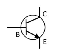
B, C, and E stand for base, collector, and emitter, respectively. The base is essentially the switch. If electrons are flowing through the base, the switch is closed and electrons are free to flow from the collector to the emitter. We can use transistors to create circuits that mimic Boolean logic.
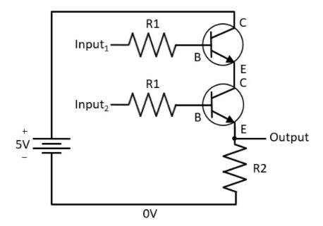
Electrons flow to the top collector, but if Input1 is 0, then electrons can’t flow, and thus the output will be 0. If Input1 is 1, then electrons flow from the emitter of the top transistor into the collector of the bottom transistor. However, if Input2 is 0, then electrons can no longer flow, and thus the output is 0. The only way the output is 1 is if Input1 and Input2 are both 1. The electrons can flow through both transistors and thus, the output is 1.
Combining transistors in this way allows us to create digital logic gates, such as AND, OR, and NOT, which are covered in the next section.
Logic Gates
Transistors make up the bulk of the digital logic gates, but if we only care about how to route 0s and 1s to perform a task, we want to look at a higher level. In other words, we don’t really care about resistors, batteries, and so forth. We just want to know, if this wire is a 1, and that one is a 0, what is the output? This is where we use logic gates to depict the task we want to perform. The term gate is meant to denote that given the right circumstances, electrons can be controlled to the output: either on or off, yes or no, true or false.
There are several ways to depict a logic circuit, including a truth table, a logic equation, a circuit diagram, or even a k-map. All depict the same information, but just in different forms. Much like how a table depicts tabular data, but a graph or chart depicts it visually. They are saying the same thing, but just in different ways.
The AND Gate
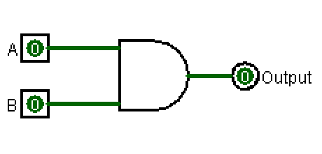
The AND gate symbol is an elongated D, and the gate itself requires A and B to both be 1 before the output is 1. This is much like how in C++, we can combine a condition with A && B, where both conditions must be true (1) for it to evaluate to true (1). Any other condition will result in it being 0. The same holds true for the AND gate.
The following truth table shows that the only way to get the output of 1, both inputs must be 1.
| A | B | Output |
|---|---|---|
| 0 | 0 | 0 |
| 0 | 1 | 0 |
| 1 | 0 | 0 |
| 1 | 1 | 1 |
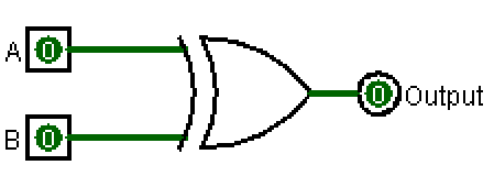
The OR Gate
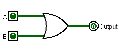
The OR gate only requires A or B (or both) to be 1 for the output to be 1. Much like in C++ you have if (A || B), only A or B or even both have to be true for the entire statement to be true.
| A | B | Output |
|---|---|---|
| 0 | 0 | 0 |
| 0 | 1 | 1 |
| 1 | 0 | 1 |
| 1 | 1 | 1 |
The NOT Gate (Inverter)
The NOT gate is a little bit different than AND or OR because it only accepts one input. That input is then inverted, meaning if it comes in as a 0, it leaves as a 1, or vice-versa.
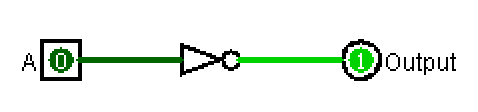
The NOT gate is actually the little circle at the end of the triangle. In fact, we can invert anything with those little bubbles. For example, I inverted one input and the output of the following AND gate, notice the location of the bubbles.
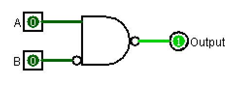
Notice the little circles for the B input and the output. Also notice that the name of the gate changed to NAND, meaning NOT AND gate. Any time we invert the output, the name of the gate changes. For example, an inverted output for the OR gate would be the NOR gate.
The Exclusive OR Gate (XOR)
The OR gate we talked about above is actually the inclusive OR gate. This gate produces a 1 only if there is 1 input with a 1. You can see that it looks much like an OR gate, except it has a second arc with the inputs.
The XOR gate has the following truth table.
| A | B | Output |
|---|---|---|
| 0 | 0 | 0 |
| 0 | 1 | 1 |
| 1 | 0 | 1 |
| 1 | 1 | 0 |
The exclusive OR is actually a combination of AND and OR gates, as you can see below.
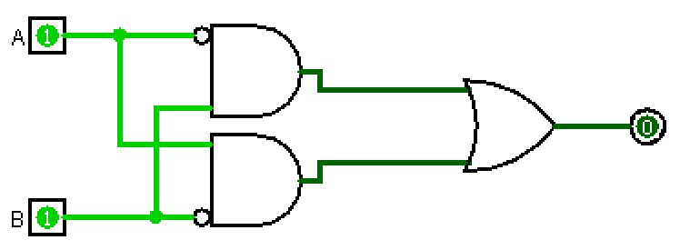
You can see we have two AND gates, where A is inverted on the top AND and B is inverted on the bottom AND. Both feed into an OR gate, which produces the output. We can actually put this in English to see how it works: “A is 0 AND B is 1 OR A is 1 AND B is 0.” Those are the only way to produce a 1. As you can see with how I configured the inputs, both inputs are 1, yet the output is 0.
Multiplexors
You can see above, we have the digital logic gates sufficient enough to make decisions. Now, what if we want to select one output or another? We can use a multiplexor, which is abbreviated MUX. The multiplexor has inputs and then a selector. The selector determines which of the inputs will become the output. This allows us to select a choice for the output.

When the selector is 0, the output takes whatever A is. When the selector is 1, the output takes whatever B is. We can use this to select an operation for a computer. For example, the following MUX selects a logical operation: AND, OR, NOT, and XOR between A and B. Since there are four operations, the selector needs to be at least two bits since: \(\log_2~4=2\).
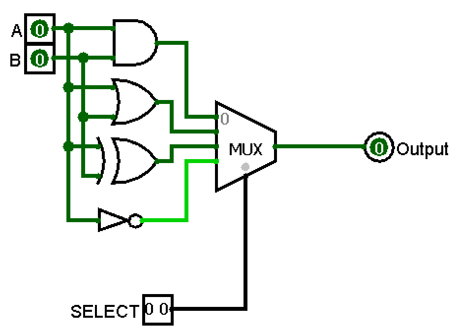
The table below shows what the output will take:
| SELECTOR | OUTPUT |
|---|---|
| 00 | A & B |
| 01 | A | B |
| 10 | A ^ B |
| 11 | ~A |
The multiplexor gives us a way to start what is starting to resemble a computer.
Combinational Logic
Combinational logic is simply “given these set of inputs, what is the output?” In other words, how can we put these logic gates together to get the output that we want.
The Adder
The most common demonstration of combinational logic is the adder. Recall from binary arithmetic that addition has two results per bits place (1s, 2s, 4s, 8s, etc.) which are the sum–the digit that goes in the place, and the carry–the digit that carries to the next place.
Here’s a truth table for binary arithmetic. Notice that there are two outputs SUM and COUT (carry out).
| LEFT | RIGHT | Carry In | SUM | Carry Out |
|---|---|---|---|---|
| 0 | 0 | 0 | 0 | 0 |
| 0 | 0 | 1 | 1 | 0 |
| 0 | 1 | 0 | 1 | 0 |
| 0 | 1 | 1 | 0 | 1 |
| 1 | 0 | 0 | 1 | 0 |
| 1 | 0 | 1 | 0 | 1 |
| 1 | 1 | 0 | 0 | 1 |
| 1 | 1 | 1 | 1 | 1 |
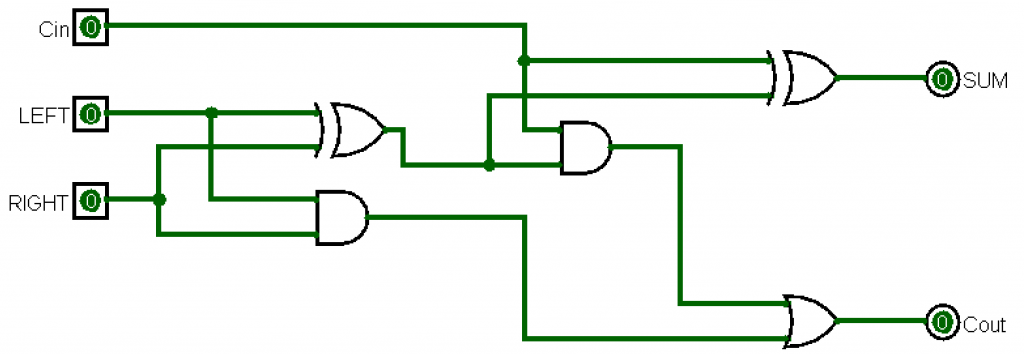
The adder above will add two bits together and produce two results: (1) the sum, which is the value for the digit’s place it is adding, and (2) the carry out, which is the value carried to the next digit’s place.
For an int, we need 32 of these chained together, for a long, we need 64 of these chained together.
Sequential Logic
Unlike combinational logic, sequential logic is “given these set of inputs AND the previous output, what is the output?” In other words, sequential logic is a way to get a circuit to remember a value. In fact, memory elements in computers are built using some form of sequential logic.
SR-latch
The central element to sequential logic is the feedback loop. As you can see with the simple SR-latch below, the output feeds back as an input to remember the previous value.
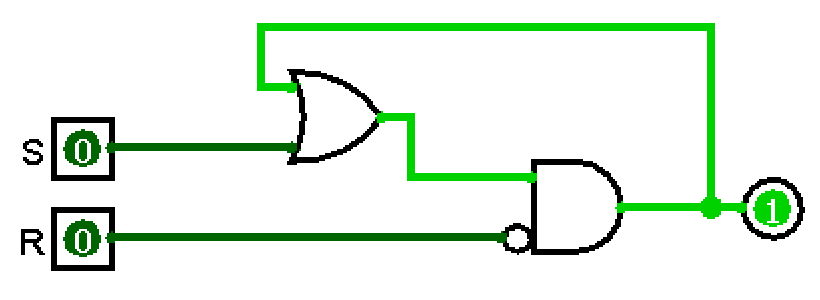
The circuit above has the following truth table.
| S | R | Output |
|---|---|---|
| 0 | 0 | Previous output |
| 0 | 1 | 0 |
| 1 | 0 | 1 |
| 1 | 1 | X |
The X in this truth table means “don’t care”. The point is that we only use the circuit for the first three rows only. If we want to remember a 1, we set S equal to 1, then set it back to 0. As long as S and R are 0, the previous output is remembered. If we want to remember a 0, we set R equal to 1, then set it back to 0.
The circuit above is called an SR-latch, since it has two inputs S (set) and R (reset). This leads to a little bit of an issue. When we write values in a computer, we only want to say “remember or don’t”. So, what if we had one pin that contains the value that we want to remember and another pin that says “remember or take the data pin”?
D-Latch
This concept is called a D-latch for data latch. In this case, we have a pin called D that contains the data (0 or 1). Then we have another pin called E for enable. If the enable pin is 0, then no matter what D is, the latch will remember the previous value. Otherwise, when the enable pin is 1, the latch will always take the value of the D pin. This is the primitive element in a computer register, which is a memory element built in the CPU.
So, instead of one pin that sets the output to 1 and one that sets the output to 0, we have one pin that contains the 0 or 1 we want to remember and one that says “remember or take the value of D”.
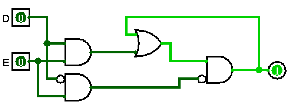
Notice that the right-hand side is the same old SR-latch that we saw above. However, the AND gates above it direct the S and R only when the enable pin is set to 1. So, if D=1 and E=1, then the top AND gate will trigger the set pin. If D=0 and E=1, the bottom AND gate will trigger the R pin, hence resetting the latch to 0. If the E pin is set to 0, then both AND gates will always output 0, hence S=0 and R=0.
There are other ways to design this latch, and in fact, most D-latch diagrams use NAND gates, such as the following D-latch. It does the same thing as above, but it uses NAND gates.
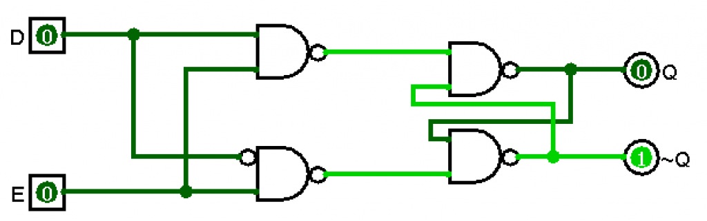
Both D-latches implement the following truth table.
| D | E | Q |
|---|---|---|
| 0 | 0 | Previous output |
| 0 | 1 | 0 |
| 1 | 0 | Previous output |
| 1 | 1 | 1 |
Flip Flops
There are two different ways we can trigger a sequential circuit to take an output, when the pin is high or low, or when the pin transitions.
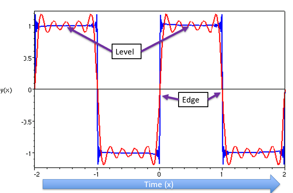
The latches we looked at are level triggered, meaning that the output will change as soon as the input changes. Flip-flops are edge triggered, meaning the output only changes on a transition. When the input goes from 0 to 1, it is called a rising edge, whereas a 1 to 0 is called a falling edge.
Registers
You can see that our D-latch and D-flip-flop (DFF) only store one bit at a time. However, the memory inside of the CPU stores much more than that. For example, on a 32-bit machine, the registers are 32 bits–that’s 32 of these put together, whereas a 64-bit machine has 64-bit registers.
A register is simply a combination of memory elements to store values. We can make a register accept one or two bits at a time, this is called a shift register, or all at once, which is the way we store values inside of a computer.
Clocking
Clocks are everywhere inside of a computer. Synchronizing data and when and at what time things occur are the only way these types of things can work. Clocking is just a fancy name for something that cycles at a particular frequency. In fact, when you buy a computer, the clock speed you see, such as 4.0GHz is the CPU clock speed. However, there are several other clocks, and that 4.0GHz is divided and multiplied throughout the whole system.
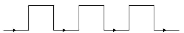
A square wave is a timing diagram that shows only two states: (1) asserted, and (0) deasserted.
This is why we refer to what we’re doing as digital logic. Digital logic is built on top of analog logic circuits, which we saw above with the transistors, resistors, and so forth. A square wave is impossible as it takes time for electrons to start flowing or to stop flowing. It happens really fast, so it seems instantaneous, much like the speed of light. So, the square wave timing diagram above is abstracted away from the actual circuit. When a bit is (1) asserted, that means electrons are flowing at a certain voltage, such as 5 volts or 3.3 volts, etc.
We use clocks because you can think of a computer much like a movie. A movie is made up of 30 pictures flashed to the screen each second to give the illusion of motion. The same thing happens in a computer, except at varying frequencies. We set all the inputs and let the electrons race their way to the output pins, we then take a snapshot of the output pins, and those are our result. We do this again after each pulse of the clock, hence creating sequencing to a computer.
Shift Registers
A shift register is also known as a SIPO or serial-in, parallel-out. It takes data in serially, meaning one bit at a time, but the way the memory elements are laid out, it has all of the pins for the taking. The following circuit is an example of a 4-bit shift register.

The shift register above has three inputs, D (data), E (enable), and a clock. The clock is meant to synchronize the four DFFs that store the data. Notice that in a shift register, the output of one DFF is the input of another. So, it will take 4 clock pulses for 4 bits to be loaded into a shift register. You can see that serial communication has far fewer wires, but in the case of a 4-bit value, it takes four times the amount of time to transmit all four bits. However, with the high clock speeds we have now, many devices have switched to serial communication, including serial ATA (hard drive communication), Ethernet (networking), and mouse/keyboard (universal serial bus or USB).
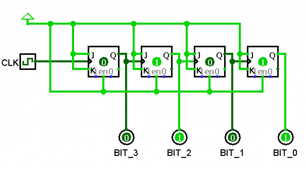
Counters
Timers are ubiquitous in a computer, and counting is very important. Most counters can be implemented using sequential logic put together, in particular, D-flip-flops.
A ring counter is a cyclical counter where a logic 1 is shifted in a ring fashion to give 4 different timing modes. This is also a way to divide a clock frequency. We can see the example of a 4-bit ring counter below.
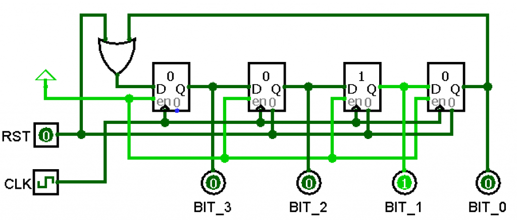
The RST resets the clock by setting all values to 0 except the first bit (BIT_3). Notice that the last bit, BIT_0, is fed into the input of the first bit, BIT_3. The CLK input is simply a square wave that keeps ticking between 0 and 1 at a certain frequency. The clock requires four pulses for the 1 to be moved across the shift registers.
You can see the counter above just moves a 1 around to essentially divide the frequency by 4, since there are four DFFs. What if we actually care about the the number? For example, if we tick the frequency 10 times, we want the counter to be 10. You can see with the ring counter, this isn’t the case.
Below, I use a JK-flip-flop, which if J=1 and K=1, then Q = ~Q. Essentially, J=1, K=1 toggles the bit. Notice that we’re using the first JKFF to pulse the clock to the other counters.
Conclusion
You can see that under the covers of digital logic are transistors and wires, typically copper or aluminum wires. What we care about is how we can route the electrons to get some meaningful result from them. We can use combinational logic to route electrons and sequential logic to remember previous results. We can calculate a variety of results and then use a multiplexor to select the result we need.
When it comes to a computer, we can think of it as a series of snapshots: set the inputs, let the electrons flow, “take a picture” of the result. Digital logic is important because it is the foundation upon which we will start building a computer.