Contents
Introduction
Computer components are not the same across all platforms. Instead, we will look at a typical programmable computer, such as the RISC-V system-on-chip (SoC). We will look at how all of these components fit together to get something happen. For example, when I type something on the keyboard, what is the chain that causes something to show up on the screen?
We will look more closely to how we develop programs in what is known as a stored program concept. We will see how the application binary interface (ABI) enforces rules that make sense for the computer architecture and make it easy for multiple languages to work together.
Memory
Memory is where we store our variables and other information. In the systems we will be talking about, we have really three forms of memory: (1) registers, (2) random access memory (RAM), (3) secondary storage (aka hard drive). Recall that registers are stored in the CPU itself, and they are the fastest, but smallest pieces of memory we have. Then, for a longer-term storage, we store what cannot fit in registers into the larger, but slower pool of memory called RAM.
RAM is usually larger, but slower than registers, but it is still volatile. This means that whenever power is no longer applied to the RAM bank, the data is lost. This is due to the design of RAM, and it can be a helpful tool. For example, when someone says, “have you tried turning it off and back on?”, that will refresh the data to a known point. Data does get corrupted sometimes by signaling and communications errors.
Since RAM and registers only store data when electricity is provided, we can use the third type of storage, a hard drive, to store data long-term. The hard drive is an order of magnitude slower than RAM, which in turn is an order of magnitude slower than registers. So, we don’t want all of our data sitting on the hard drive that we might need sooner than later.
Have you ever loaded a program and it sits at a screen “loading…” or something like that? The operating system is responsible for loading the executable program into memory before running it. However, sometimes we need additional data from the hard drive. This is where files come into play. A file is a section of memory on a hard drive that contains data, such as a music file, a picture, or a word document.
Registers
Recall that registers are small pieces of memory built into the CPU itself. When we say we have a “64-bit” computer, we mean that the registers inside of the CPU of that computer can store 64 bits (8 bytes) of information. The registers trade size for speed. Registers are one of the most (if not THE most) speedy pieces of memory we have inside of our system.
Most reduced instruction set computers (RISC) utilize a load/store architecture. This means that the CPU’s arithmetic and logic unit (ALU) as well as the floating-point unit (FPU) can only operate on data from registers or from small immediates built into the instruction itself. This means that if we want to add two pieces of data from RAM, we will first load them from RAM into registers before we add them.
The load/store architecture makes it simple to know when we’re using registers and when we’re using RAM. If we are using a load or store instruction, such as lb, lh, or sw, sd, then we know that we’re going to RAM, and we will suffer a timing penalty for doing so.
Random Access Memory (RAM)
Random access memory is an all-encompassing term to refer to a longer term, volatile storage area in a computer. When we buy RAM for our laptops or PCs, we buy what is known as dynamic RAM. Some computers, such as mobile phones or console gaming platforms, use static RAM.
Static RAM (SRAM)
Static RAM uses the sequential logic we looked at earlier. Static RAM uses several transistors to statically lock in a value by feeding back the previous output as an input to a logic circuit. These can be stored using latches or flip-flops. Static RAM is stable and it is fast. However, it requires a lot of transistors just to store one bit!
Dynamic RAM (DRAM)
Since RAM started growing rapidly, storing one bit needed to use far fewer logic gates meaning fewer transistors. Dynamic RAM solves this issue at the expense of other things we will discuss a little bit later. DRAM uses a capacitor (called a trench capacitor) to store a bit’s value and one transistor to control the capacitor.
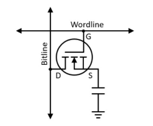
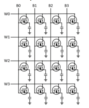
These storage elements store one bit at a time. We can arrange them in a grid to store multiple words.
Dynamic RAM works by storing one bit inside of a capacitor. If the capacitor is charged, we stored a 1, and if the capacitor is discharged, we stored a 0. Far fewer components are needed to store one bit using dynamic RAM. This is the main advantage. We can squeeze several bits in a much smaller space using this scheme. This is why buying 16, 32, 64, or even 128 gigabytes (16, 32, 64, 128 billion bytes) relatively cheaply and with the same form factor we used to store 2 or 4 megabytes of information.
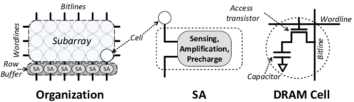
Dynamic RAM is laid out in grid form, meaning it has a row and a column. How the rows and columns correspond to the memory address is up to the memory module, but we can use a simple method like taking the upper word as the row and the lower word as the column. For example, 0x1234_ABCD would be at row 0x1234 and column 0xABCD.
If we examined what is at a row and a column, we would find a subarray, which is just a set of bits. This set of bits is called a word.
Using dynamic RAM introduces several problems:
- Capacitors leak their charge over time. Since the capacitors used in DRAM are extremely small, they do not store a lot of charge. This means that the charge leaks fairly quickly–sometimes tens of milliseconds. The memory controller is required to put the value back into the capacitor at regular intervals. These period intervals are commonly referred to as refresh cycles.
- Reading a value from a capacitor discharges it. This means that when we read a value, we actually destroy that value in the RAM bank. So, after reading a value, the memory controller is required to put back the value.
- Charging a capacitor is not instantaneous. It takes time to charge a capacitor from no charge to full charge. DRAM has gone through several changes, but the voltage around 2007-era in the capacitors was around 1.80V-1.50V. This was reduced by better components and some design changes to around 1.40-1.20V in the 2020-era.
- These capacitors store a very small amount of charge. Therefore, we need a device called a sense amplifier to amplify the charge so that we can send it to the CPU.

Random access memory banks are physically located away from the CPU. This introduces a physical limitation. The following picture shows an AMD motherboard with four banks of RAM slots (RAM is not present in the slots).
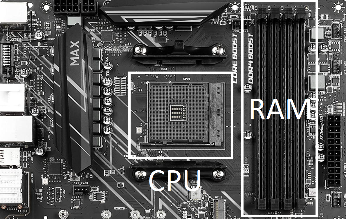
They seem close to us, but with the frequencies we are pushing now, the physical distance between components makes a lot of difference. This means that no matter what we do, the difference in speed between the CPU registers and RAM means that going out to RAM is order of magnitudes slower than just working with registers. However, we need RAM because of its size. This motivates the use of cache, which we explain later in this chapter.
Double Data Rate (DDR)
There is a memory controller and a memory module controller. The CPU contains the memory controller, and it’s responsible for getting or setting the bytes requested by the CPU (during a load/store). However, with the complex circuitry necessary to store bits, refresh the RAM, and so forth, there is a controller in the memory bank. The term data rate refers to the speed at which the memory controller and memory module can transfer data.
Prior to DDR, the memory controller could send a word or receive a word in one clock cycle. DDR improved upon this by allowing transfers at the rising-edge AND falling-edge of a clock. Hence, we now get two transfers within one clock cycle.
If you go to buy RAM nowadays, you will see several numbers, including clock rates, and timing characteristics:
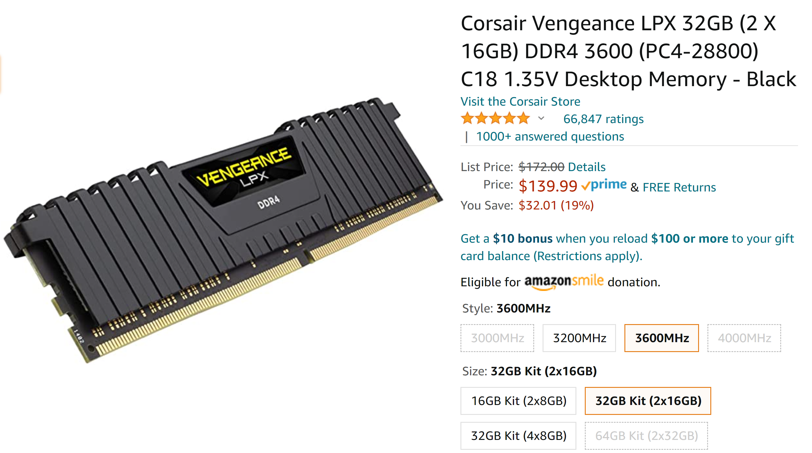
You can see that we have an option to buy 3000 MHz (3 GHz), 3200 MHz, 3600 MHz, and 4000 MHz RAM. This is the clock rate at the memory module. Since this is DDR4 memory, this means that we can transfer data at a rising edge and falling edge of a clock, meaning we can transfer 3 – 4 billion words in one clock cycle.
DRAM Timings
If we look even closer at the memory module, we see a timings grid, which describes the timings of the individual memory module.
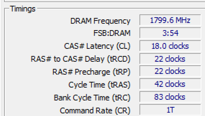
The DRAM frequency is the clock speed. Since this is DDR4 memory, we double that. So, you can see that in my personal computer, my memory speed is 3600 MHz (1800 MHz doubled). The FSB:DRAM is the front-side bus to DRAM ratio. The front side bus is the communication port of the CPU. For every three cycles of the clock of that bus, the memory clock will cycle 54 times.
We then have the timings CL, tRCD, tRP, tRAS, tRC, and the command rate (CR). When looking at the timings, recall that DRAM is ordered in rows and columns.
- CL is short for CAS Latency, which means column address strobe latency. This is the number of clock cycles required to wait before a word is ready to be read by the memory controller after the CPU selects a memory address to be read from or written to. The memory address is broken up into a row and a column. So, the memory controller will select the row, and then send the column. The CAS is how long the memory controller now has to wait before reading the data.
- tRCD is short for row address (RAS) to column address (CAS) delay. The memory controller will send which row it wants to read to the memory module. Afterward, it will send out the column it wants to read. However, the memory controller must wait tRCD clock cycles between the row and the column.
- tRP is short for row precharge time. When the memory controller selects a row, it will physically drive a wire up or down (voltage on or voltage off). Since we’re dealing with complex circuitry, before selecting another row, the memory controller must wait tRP clock cycles. This is because selecting a row after another row is not instantaneous.
- tRAS is short for row address strobe. This is the amount of time that the row has to have been selected before it is considered valid.
- CR is short for command rate. The command rate is the number of clock cycles required to select a RAM bank before sending a command. The command rate is usually 1, 2, or 3, meaning that it will take 1, 2, or 3 clock cycles to consider a RAM bank selected. Notice that there are four slots in the motherboard shown above. The command rate is the number of cycles needed to select one of those slots. The number of cycles usually depends on the physical distance of the slots from each other, and the “cheapness” of the components used to make up the circuit board in the memory itself.
There are many other clock timings in RAM, but the last one that is not in the graphic, which is important, is the tRFC, which is the row refresh cycle time. This is the number of clock cycles to wait before considering a row refreshed. Recall that we have to refresh a row because the capacitors lose charge over time and need to have their values put back into them, which we are calling refreshed.
Cache
Registers are very fast, but very small, and RAM is very slow, but very large. This large discrepancy makes loads and stores untenable in many situations. The CPU will have to sit and wait for the RAM to be loaded or stored before it can continue to do other things. Also, remember that instructions are stored in RAM!
Surely there’s a better way. This is where cache comes into play. Cache is something that is placed in between CPU registers and RAM. We can even have multiple levels of cache. For example, the Intel i7 I’m writing this on has 3 levels of cache, whereas the laptop I have only has 2 levels of cache.
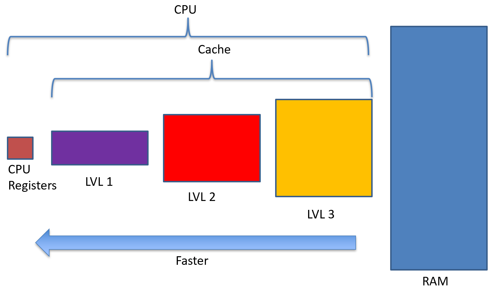
Cache is usually built into the CPU itself, which also contains the memory controller. So, when we load or store a value from memory, the address is first searched in level 1 cache, if it isn’t there, then level 2 cache is searched, then if it isn’t there, level 3 cache is searched. Finally, if the value cannot be found in cache, the CPU will ask the memory controller to go out to RAM to load the value.
When the value searched for is NOT in cache, we call this a cache miss. When the value searched for is in cache, we call this a cache hit. We are trying to increase the number of hits and decrease the number of misses. This comes into the design decisions when architecting cache.
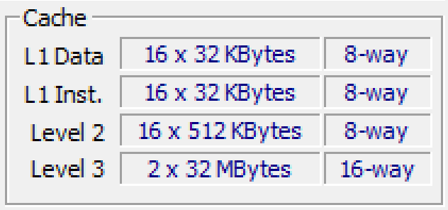
My personal computer has the following cache configuration as an example.
Principle of Locality
Cache is a smaller set of the larger RAM memory. We are trying to increase the number of cache hits and decrease the number of cache misses. We can use a little bit of psychology to see how a programmer writes their program to exploit what is known as locality. There are two principles of locality: (1) principle of spatial locality and (2) principle of temporal locality.
We can exploit temporal locality by only placing those memory addresses and values that we use over and over again in cache. Recall that cache is smaller than RAM, and hence, it can only store a much smaller subset of RAM.
We can exploit spatial locality by grabbing more than just the value we’re looking for. In fact, cache has a block size, which is the number of bytes surrounding the value we’re looking for. For example, if we have a sixteen-byte block size, and we request a word (4 bytes), then 3 additional words are stored in cache around the original word we’re interested in.
We will look at three ways to organize how an address maps to cache: (1) direct-mapped, (2) set-associative, and (3) fully associative.
Three Cs of Cache Misses
A compulsory miss occurs the first time we access the memory address. Since cache is generally reactive, it can only place things in cache that we’ve already requested. We can reduce compulsory misses by allowing speculation or prefetching, which means we store things into cache that we think might be needed in the near future. Since prefetching can help mitigate compulsory misses, increasing the block size would mean that when a value is prefetched, more data comes with it. This increases the chances that the next memory access will contain the prefetched value.
A capacity miss occurs when there is no more room in cache to store what we’ve just requested. In this case, we need to evict an entry based on the eviction policy (also known as cache replacement policy). We can reduce capacity misses by increasing the cache size.
A conflict miss occurs when two memory addresses map to the same location. We can reduce conflict misses by increasing the associativity of the cache.
Direct-mapped Cache
Since cache is smaller than memory, we have to determine how addresses will map to locations in cache. There is another tradeoff we have to consider here. If we have a simple map, such as “take the last three bits of the address”, then this is a constant time operation (known as O(1)). That is, the find the address in cache that this memory address maps to takes just as long as it takes to make the arithmetic calculation. However, this may waste space in cache if more and more addresses map to the same location.
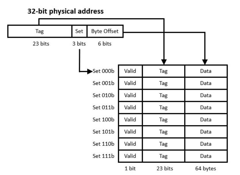
In the figure above, we can see that the memory address is split into the tag, set, and byte offset. We can recreate certain things here. For example, the byte-offset is 6, meaning that our block size is \(2^6=64~\text{bytes}\). The set is three bits, which tells us which set to go into. Finally, the tag is the portion of the memory address we cannot recreate with the set and the byte offset.
Direct-mapped cache uses a set-function to determine which set a RAM memory value will be placed in cache. This means that all addresses can be known ahead of time
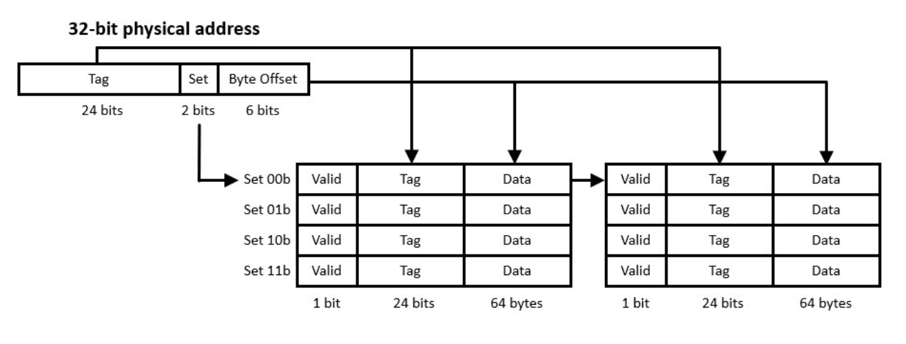
Set-associative Cache
Fully-associative Cache
All the caches that we looked at above uses a portion of the address to push them into a particular set. However, if all of the addresses keep mapping to the same sets, we could waste cache space by not having addresses that map to unused sets. So, instead of breaking apart our cache into sets, we can have one superset and instead, break the cache into many ways. This means that the full size of the cache is always utilized.
Fully-associative cache can nearly eliminate conflict misses as long as it is large enough. However, the circuit complexity increases, and implementing fully-associative cache over direct-mapped cache means more transistors, more logic, and more headaches.
Split Cache
RAM is just a large piece of memory, and so is cache. However, sometimes we want to prefetch on instructions but maybe not on data. In some circumstances, the system can implement a split cache. This means that we have two caches: (1) one for data and (2) one for instructions. These are called D-cache and I-cache, respectively.
Eviction Policies
Any associative style cache, such as set-associative or fully-associative cache, requires that it decides which entry needs to go due to a capacity miss. To make sure we’re fully utilizing locality, we can implement eviction policies such as first-in, first-out (FIFO), least recently used (LRU), and least frequently used (LFU). There are others, but these are the policies I want you to be familiar with.
First-in, First-out (FIFO)
The FIFO policy will evict the oldest entry that made it into cache. This is very simple to implement if we store when the entry was added into cache. The problem is that we could still be using a cache value over and over again that just so happens to be the oldest. In this case, we would evict a memory address and suffer a miss even if we are still using it.
Least Recently Used (LRU)
The LRU policy will evict those entries that haven’t been used in a while. This implies the concept of time. This policy requires that we store the time since it was last accessed (read or written).
Least Frequently Used (LFU)
The LFU policy will evict those entries that haven’t been frequently used. This policy requires that we store the number of accesses (read and writes) to the cache entry. The entry with the fewest accesses will be evicted during a capacity miss.
Write Policies
We have one final decision to make. When a value is written, do we write only to cache or do we write all the way back to RAM? There are two write policies we can implement: (1) write back and (2) write through.
The write back cache policy will only write the most recent cache value back to RAM (and higher cache levels) during an eviction. This means that RAM and higher cache levels will contain an older value, and hence, it will no longer represent the latest memory value that we’re looking for. Write-back is fine as long as we’re using the same CPU or CPU core for all reads and writes. However, what if another core wants to access the same memory location? In a write back policy, we will no longer have cache coherency. That is, two cores will have a different view of memory. We can design more complex logic to permit snooping, where one CPU snoops on another’s CPU cache. Bottom-line: the write back cache policy favors speed over synchronization.
The write through cache policy will write the value to cache and through all higher levels of cache and eventually through to RAM. There is no need to implement snooping or other complex logic. Bottom-line: this write through cache policy favors synchronization over speed.
Memory Management Unit (MMU)
The memory management unit’s job is to translate virtual memory addresses (VMA) into physical memory addresses (PMA). The structure of how the MMU does this is based on the architecture; however, most follow a basic way to translate addresses by using page tables.
The memory management unit I will discuss here is the RISC-V Sv39 MMU. This MMU takes 39-bit virtual addresses and produces a 56-bit physical address. The process for doing so requires some discussion.
All page tables are stored in normal RAM. The operating system is responsible for placing the tables in RAM and writing the values it wants into the tables themselves. A page table is made up of 512 page table entries (PTEs) and each entry is exactly 8 bytes. So, each table takes exactly 4,096 bytes (4KiB).
Virtual Memory
We’ve been lying to you this whole time. Whenever you load and store from and to a memory location, the memory location isn’t real! These memory locations are called virtual memory locations, which get translated into a physical memory location using a logic device called the memory management unit (MMU).
The operating system is responsible for programming the MMU. Luckily for you, I won’t make you do this until you sign up for my operating system’s course. We just want to know the basics. However, I will have you pretend to be the MMU and translate a virtual memory address into a physical memory address. Each architecture has its own MMU scheme. For this lecture, we will be using the RISC-V architecture’s SV39 (39-bit virtual address) scheme. This scheme translates a 39-bit virtual address into a 56-bit physical address.
The Memory Management Unit
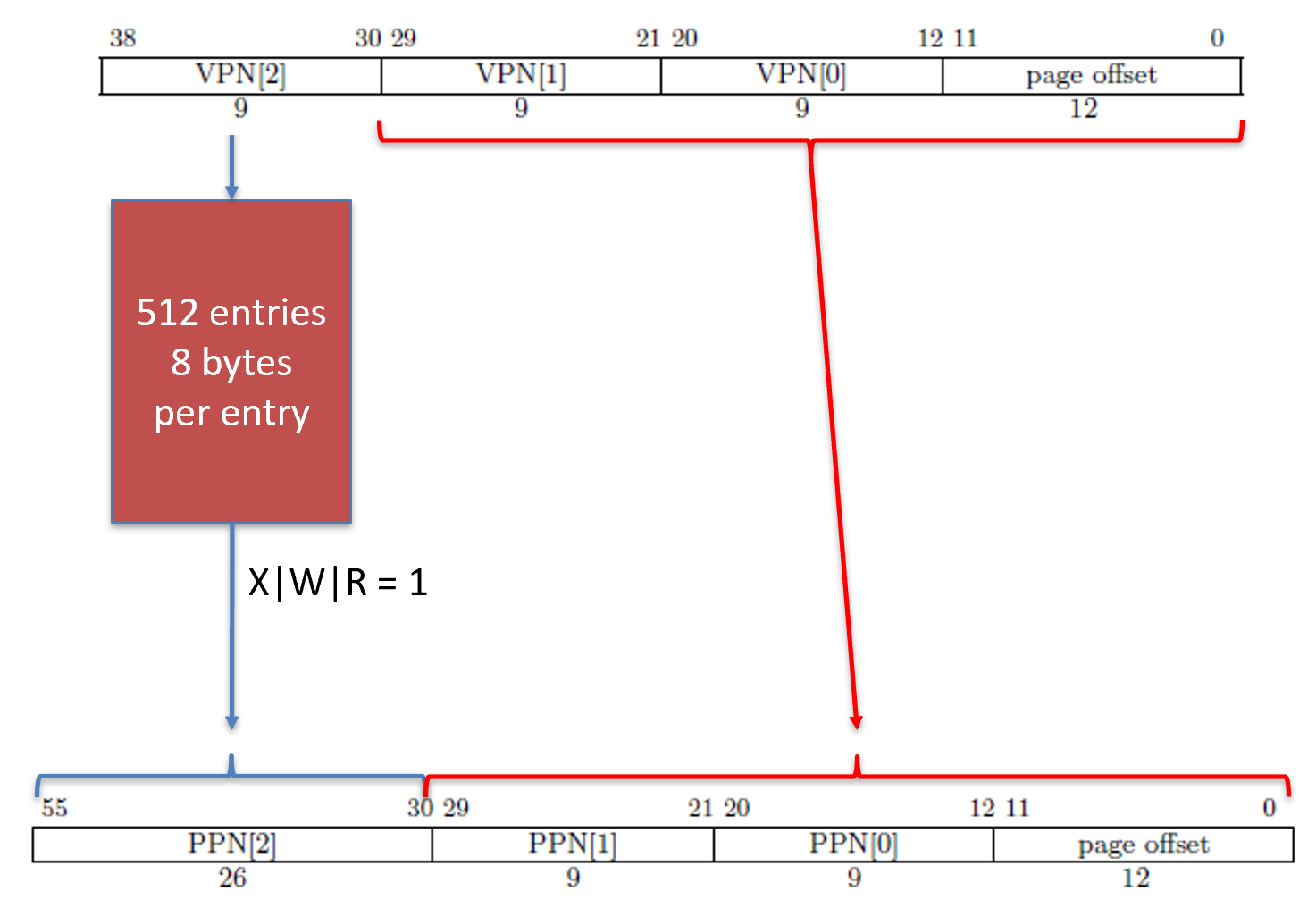
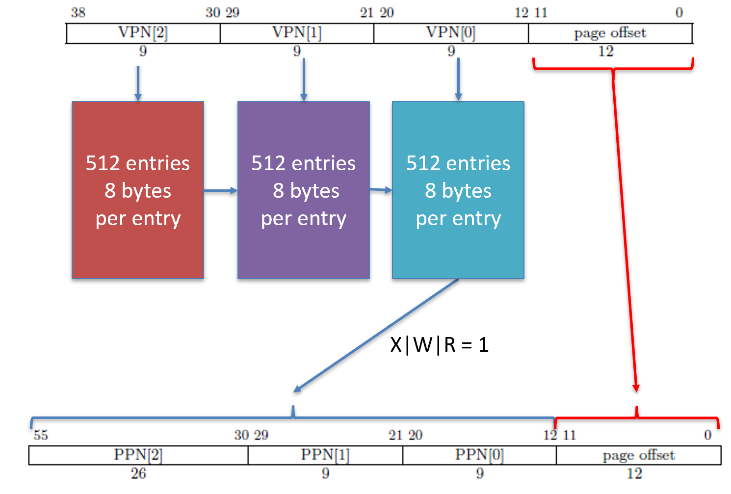
The memory addresses we load from and store to are virtual memory addresses. A virtual memory address has nothing to do with where a value is located in physical memory. Instead, the virtual memory address contains indices which tells the MMU where to look when translating the address into a physical memory address. The RISC-V Sv39 scheme splits a virtual memory address into the following fields.
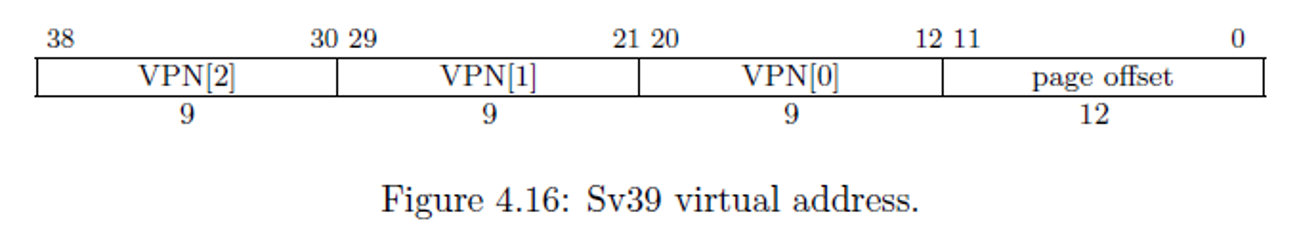
Notice we have VPN[2], VPN[1], and VPN[0]. VPN stands for virtual page number. The value (2, 1, and 0) refers to level 2, level 1, and level 0. Yes, we have a maximum of three levels of page tables. These are indices into an array that stores 512-entries. This is why we have 9 bits: \(2^9=512\). When the MMU is finished, it produces a physical address that looks as follows.
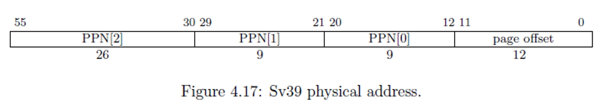
The physical address, when spliced together, is the actual location in RAM where we look for a value.
Translating Virtual Addresses
To get from the virtual address to the physical address, we use the memory management unit (MMU). The memory management unit uses the following flowchart to translate:

Page Tables
The memory management unit starts to translate by using page tables. These tables contain 512 page table entries. Each entry has the following format (remember, there are 512 of these).

Each page table entry is 8 bytes (64 bits), so \(512\times 8=4096\). Each table is exactly 4,096 bytes (4KiB). This size will come up a lot in the MMU, so don’t confuse them!
There are several bits here, including V, R, W, X, and so forth. The bits from left-to-right are: Valid, Read, Write, eXecute, User, Global, Accessed, and Dirty. The valid bit must be 1 for the entry to be considered valid. Otherwise, the MMU will cause a page fault. The RWX bits represent the permission of the memory addresses pointed to by the page table entry. If the R bit is set, then the load instruction is permitted to read from this memory location. If the W bit is set, then the store instruction is permitted to write to this memory location. If the X b it is set, then the instruction fetch cycle is allowed to retrieve an instruction from this memory address. Otherwise, if an operation is NOT permitted, then the MMU will cause a page fault. The last permission bit is the User bit (U). The memory is split into two sections: (1) system and (2) user. The system memory belongs to the operating system. If the U bit is equal to 0, then only the operating system can access the memory location. Otherwise, user applications are permitted to access the memory location, provided the RWX bits are set appropriately.
PPN is in different locations!
Notice that we have PPN[2], PPN[1], and PPN[0]. These correspond to the same names in the physical memory address. However, the confusing part is that in the page table entry PPN[0] is at bit 10, but in the physical address, PPN[0] starts at bit 12. This means that they don’t line up exactly, so there is some shifting that you must do before you form the physical address.
These page tables are located in RAM. However, notice that only bits 12 through 55 contribute to the page table’s location in RAM. This means that the last three hex digits of where the table is located must be 0s. Therefore, 0xabcd_ef01 is NOT an appropriate memory address, but 0xabcd_e000 is. Recall that each hex digit is 4 bits, so \(4\times 3=12\). Funny enough, \(2^{12}=4096\). I told you this number would come up over and over again!
Supervisor Address Translation and Protection Register (SATP)
The MMU has a known starting point. This is a register called the supervisor address translation and protection (SATP) register. Since page tables can be located anywhere in RAM (given the last three hex digits are 0), the MMU has to have a defined starting point, and the SATP register is it!
The SATP register contains three fields and is described below.
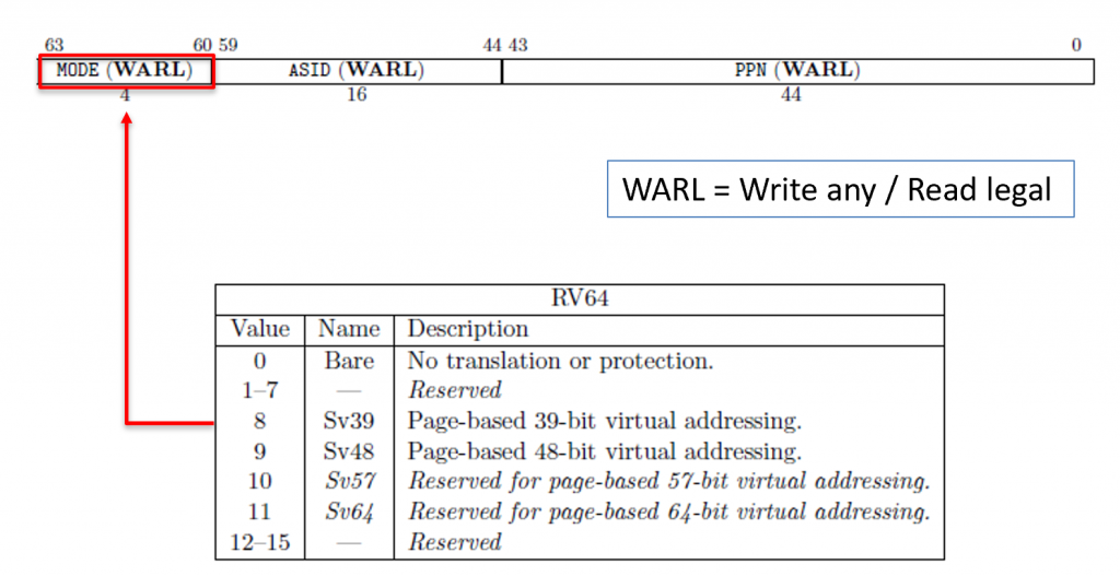
The three fields are: (1) mode, (2) address space identifier (ASID), and (3) physical page number (PPN).
The MODE Field
Only the operating system is permitted to write to this register. The MODE field determines if the MMU is turned on or off. If the MMU is turned on, the MODE determines what scheme the MMU will use. Here are the different modes.
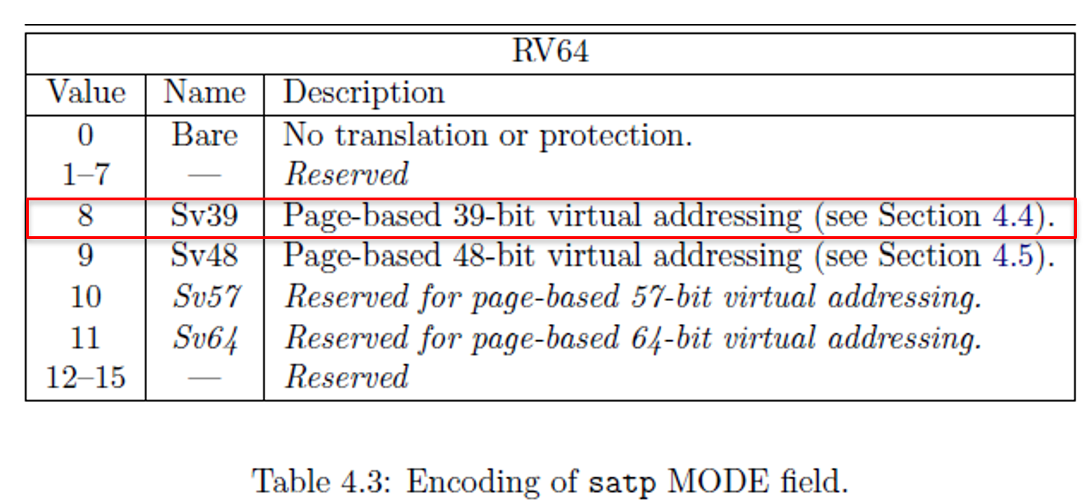
You can see that if the operating system sets the MODE field (upper four bits of the SATP register) to 0, the MMU is turned off. Otherwise, if the operating system sets it to 8, then the MMU will use the Sv39. This is a specification, and not all MMUs support all modes.
The ASID Field
The address space identifier (ASID) is used to tag the translation look-aside buffer (TLB) entries. The TLB is described more below, but the reason we do this is because every time we change the SATP register, we don’t want to flush out the cache (TLB). The operating system, instead, can put a value in ASID so the MMU knows who is using the MMU. When the MMU searches the TLB, it only matches those who match the ASID. Everyone else is ignored.
The Physical Page Number (PPN) Field
The physical page number (PPN) is where the first level (level 2) page table is located. Do NOT confuse this with PPN[2..0] in the page table entry, this is NOT the same thing. Instead, this is a physical memory address where the first page table can be located. However, notice that the PPN only stores 44 bits. Recall that the last 12 bits (last 3 hex digits) must be 0. So, instead of wasting space in the register to store these 12 0s, we store the physical address without these 0s. So, when we store the physical address of level 2’s page table, we first shift the address right by 12 places.
When the MMU wants to find the level 2 page table, it will take the PPN and shift it left by 12 places (adding 3 hex 0s to the right of the address), which makes a 56-bit physical address. Recall that all physical addresses in the Sv39 scheme are 56 bits. This physical address is where the level 2 page table starts.
Virtual Page Numbers (VPN)
The MMU has tables that contain 512 page table entries (PTEs). So, when we get VPN[2], that’s just an index into the level 2’s page table. Recall that each entry is exactly 8 bytes, so the MMU will first go to the SATP and grab PPN. It then shifts this PPN left by 12 places and adds VPN[2] times 8. Then, we can dereference this memory address and grab an 8-byte PTE.
$$PTE_{2}=(PPN_{\text{SATP}}<<12)+VPN_2\times8$$
In other words, to get a single entry from the 512 entries at level 2, we take the PPN from the SATP register, shift it left by 12 places, then add VPN[2] times 8. We multiply VPN[2] by 8 because each PTE is exactly 8 bytes.
Decoding the Page Table Entry (PTE)
When we dereference the memory address above, we get an 8-byte PTE. The MMU will first check the V (valid) bit. If this bit is 0, then the MMU can’t continue translating, and it will tell the CPU that the load/store/IF caused a page fault. Typically, your user application will print “Segmentation fault” and your application will crash whenever the MMU signals a page fault.
After checking the V bit, the MMU will check the RWX bits. If all three of R, W, X are 0s, then this entry is called a branch. The following chart describes what each RWX means.
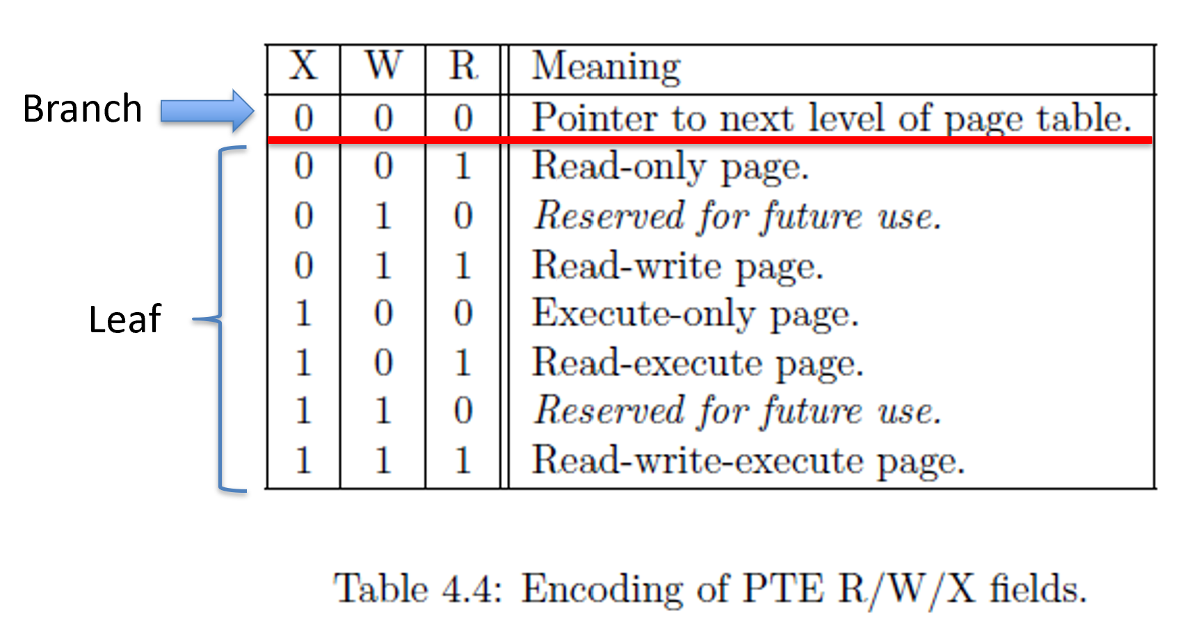
A branch means that we have yet another level of page tables to continue translation. A branch’s PPNs describe where to find the next page table (much like PPN in the SATP register). A leaf means that the page table entry contains the physical address to translate into.
Decoding Branches
Recall that a branch has the RWX bits set to 0. Then, we take PPN[2..0] and shift them into the physical memory address’ correct locations (bits 55 through 12). Notice that in the PTE it uses bits 53 through 10, so some shifting is in order! Whenever we form this new physical address, this is where in RAM the next level’s (level 1) page table is located. Whenever we get this memory address, we then take \(\text{PTE}_1=(PPN_2 << 30 | PPN_1 << 21 | PPN_0 << 12)+VPN_1\times 8\).
When we dereference this formed memory address, we will have \(\text{PTE}\) at level 1. Again, we look at the V (valid) bit, then the RWX bits, and do the same thing over and over again. If this is a branch, we have YET ANOTHER page table. Yes, there are a maximum of three page tables.
Decoding Leaves
Recall that we can have a leaf at level 2, level 1, and level 0. We can detect a leaf if RWX or any combination thereof are 1. When we have a leaf, we have to copy some portions of the PTE and some portions of the virtual address to form the final physical address. Each level determines how much comes from the virtual address and how much comes from the PTE to form the physical address.
| Leaf at Level | PPN[2] in PA | PPN[1] in PA | PPN[0] in PA | PO in PA | Resolution |
|---|---|---|---|---|---|
| 2 | PPN[2] in PTE | VPN[1] in VA | VPN[0] in VA | PO in VA | 1GiB |
| 1 | PPN[2] in PTE | PPN[1] in PTE | VPN[0] in VA | PO in VA | 2MiB |
| 0 | PPN[2] in PTE | PPN[1] in PTE | PPN[0] in PTE | PO in VA | 4KiB |
If we have a leaf at level 2, then only PPN[2] comes from the page table entry. We copy VPN[1] directly into PPN[1], VPN[0] directly into PPN[0], and the page offset becomes the last 12 bits of the physical address. However, if we have a leaf at level 1, then PPN[2] and PPN[1] come from the page table entry, where as VPN[0] copies into PPN[0] and PO copies into the page offset.
Having a leaf at level 2 means that the MMU only translates to the nearest gigabyte (1GB). Everything else is copied directly from the virtual address. Having a leaf at level 1 means that the MMU only translates to the nearest 2 megabytes (2MB). Everything else is copied directly from the virtual address. Finally, having a leaf at level 0 means that the MMU only translates to the nearest 4 kilobytes (4KB). The page offset (last 12 bits) are copied directly to the physical address.
Address Resolution
If we have a leaf at level 2, then that entire 1GiB (1,073,741,824 bytes) range will have the exact same read, write, execute, and user permissions. We don’t often see 1GiB page entries because this wastes a lot of space. The reason the address resolution is so poor is because only VPN[2] gets translated into PPN[2]. Everything else is copied from the virtual address, including VPN[1], VPN[0], and the page offset directly into PPN[1], PPN[0], and page offset of the physical address respectively.
If we have a leaf at level 1, then the entire 2MiB (2,097,152 bytes) address range will have the exact same read, write, execute, and user permissions. As with the 1GiB, the 2MiB page entries also waste quite a bit of space and aren’t widely used. Unlike a leaf at level 2, a leaf at level 1 will translate VPN[2] into PPN[2] and VPN[1] into PPN[1]. Everything else, including VPN[0] and the page offset are directly copied from the virtual address into the physical address.
If we have a leaf at level 0, then the entire 4KiB (4,096 bytes) address range (0xyyyyy000 through 0xyyyyyfff) will have the same read, write, execute, and user permissions. A 4KiB page is the most common page resolution. Recall that we can still narrow down to one byte by copying the page offset from the virtual address directly into the physical address. A leaf at level 0 means VPN[2], VPN[1], and VPN[0] are translated into PPN[2], PPN[1], and PPN[0], respectively. The only part of the virtual address copied into the physical address directly is the page offset.
Translation Look-aside Buffer (TLB)
The TLB is just a small piece of memory that keeps track of the most recent translations. Notice that when we use a pen and paper, it takes us a while to translate a virtual memory address into a physical address. The MMU takes quite a bit of time too (relatively). The TLB stores a virtual address and a physical address. So, when translating a virtual address, the MMU can look in the TLB first. If the virtual address is in the TLB, then it’s a direct lookup to get the physical address. If the virtual address IS NOT in the TLB, then we have to walk the page tables.
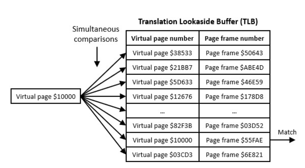
The TLB is essentially cache. Instead of walking the page tables, it is a direct lookup. However, for the simultaneous comparisons to be made without exploding the TLB design, the TLB must be rather small compared to the set of RAM addresses. Just like cache, conflicts can arise and evictions must occur.
Practice (4KB)
I wrote an MMU simulator for practice. Head on over to: https://web.eecs.utk.edu/~smarz1/courses/cosc230/mmu.
At the top, enter the problem ID 1.
You can type a memory address or SATP to dereference that given memory address or SATP register.
We are the MMU for these problems. So, for problem ID 1, we will translate the virtual memory address 0xdeadbeef. This memory address is used quite a bit as a joke and used for debugging purposes, but it’ll serve our needs here.
- Get the value of the SATP register. Check the mode to see if the MMU is turned on. Then shift PPN left by 12 places.
- SATP is 0x8000000000123456
- MODE = 8 (Sv39)
- ASID = 0
- PPN = 0x123456000
- Decompose the virtual address into VPN[2], VPN[1], VPN[0], and PO.
- 0xdeadbeef is 0b11[01_1110_101][0_1101_1011]_[1110_1110_1111]
- The square brackets [] show where the VPNs and PO are broken apart into.
- VPN[2] = VADDR[38:30] = 0b11 x 8 = 0b0000_0001_1000 = 0x018
- VPN[1] = VADDR[29:21] = 0b0_1111_0101 x 8 = 0b0111_1010_1000 = 0x7a8
- VPN[0] = VADDR[20:12] = 0b0_1101_1011 x 8 = 0b0110_1101_1000 = 0x6d8
- For all VPNs, if we add three 0s to the end of the binary number, that’s the same as a left shift by 3 places.
- A left shift by three places is the same as multiplying by \(2^3=8\).
- PO = VADDR[11:0] = 0xeef
- 0xdeadbeef is 0b11[01_1110_101][0_1101_1011]_[1110_1110_1111]
- Place the 0x018 we got for VPN[2] x 8 into the PPN (0x123456018)
- Dereference 0x123456018 to get PTE at level 2.
- This gives us 0x0000000000774101
- Check to see if it is valid (V bit = 1). Ours is 1, so it is valid.
- Check if this is a leaf or a branch.
- Our R, W, and X bits are all 0, this is a branch.
- Grab PPN[2], PPN[1], PPN[0] shift them into the correct location.
- 0x774101 is 0b0111_0111_0100_0001_0000_0001
- PPN[0] starts at bit 10: [0b0111_0111_0100_00]01_0000_0001
- 0b[0111_0111_0100_00]_0000_0000_0000 = 0b0001_1101_1101_0000_0000_0000_0000
- = 0x1dd0000 + VPN[1] x 8 = 0x1dd07a8
- Dereference 0x1dd07a8 to get PTE at level 1.
- This gives us 0x0000000000002001
- Again, check the valid and RWX bits. Ours is valid and is yet another branch (RWX all equal 0).
- 0x2001 = 0b0010_0000_0000_0001
- PPN[0] starts at bit 10: 0b[0010_00]00_0000_0001
- Add 12 zeros: 0000_1000_0000_0000_0000 = 0x08000
- 0x8000 + VPN[0] x 8 = 0x86d8
- Dereference 0x86d8 to get PTE at level 0.
- This gives us 0x000000000001700f
- Yet again, check the valid and RWX bits. Ours is valid and RWX are all set, this is a leaf. IF this was a branch, there are no more levels, and the MMU would page fault.
- Shift PPN[2], PPN[1], and PPN[0] into place and copy the page offset from the virtual address (0xeef).
- Remember, a leaf at level 2 only uses PPN[2] here, everything else is copied from the virtual address.
- Remember, a leaf at level 1 only uses PPN[2] and PPN[1] here, everything else is copied from the virtual address.
- 0x1700f = 0b[0001_0111_00]00_0000_1111
- PPN[0] starts at bit 10: 0b0000_0101_1100_0000_0000_0000 = 0x05c000
- = 0x5c000 + Page Offset = 0x5ceef.
- Therefore, 0xdeadbeef (virtual) translates into 0x5ceef (physical).
Practice (2MB)
I wrote an MMU simulator for practice. Head on over to: https://web.eecs.utk.edu/~smarz1/courses/cosc230/mmu.
At the top, enter the problem ID 2.
You can type a memory address or SATP to dereference that given memory address or SATP register.
We are the MMU for these problems. So, for problem ID 1, we will translate the virtual memory address 0xdeadbeef. This memory address is used quite a bit as a joke and used for debugging purposes, but it’ll serve our needs here.
- Get the value of the SATP register. Check the mode to see if the MMU is turned on. Then shift PPN left by 12 places.
- SATP is 0x8000000000123456
- MODE = 8 (Sv39)
- ASID = 0
- PPN = 0x123456000
- Decompose the virtual address into VPN[2], VPN[1], VPN[0], and PO.
- 0xdeadbeef is 0b11[01_1110_101][0_1101_1011]_[1110_1110_1111]
- The square brackets [] show where the VPNs and PO are broken apart into.
- VPN[2] = VADDR[38:30] = 0b11 x 8 = 0b0000_0001_1000 = 0x018
- VPN[1] = VADDR[29:21] = 0b0_1111_0101 x 8 = 0b0111_1010_1000 = 0x7a8
- VPN[0] = VADDR[20:12] = 0b0_1101_1011 x 8 = 0b0110_1101_1000 = 0x6d8
- For all VPNs, if we add three 0s to the end of the binary number, that’s the same as a left shift by 3 places.
- A left shift by three places is the same as multiplying by \(2^3=8\).
- PO = VADDR[11:0] = 0xeef
- 0xdeadbeef is 0b11[01_1110_101][0_1101_1011]_[1110_1110_1111]
- Place the 0x018 we got for VPN[2] x 8 into the PPN (0x123456018)
- Dereference 0x123456018 to get PTE at level 2.
- This gives us 0x0000000000774101
- Check to see if it is valid (V bit = 1). Ours is 1, so it is valid.
- Check if this is a leaf or a branch.
- Our R, W, and X bits are all 0, this is a branch.
- Grab PPN[2], PPN[1], PPN[0] shift them into the correct location.
- 0x774101 is 0b0111_0111_0100_0001_0000_0001
- PPN[0] starts at bit 10: [0b0111_0111_0100_00]01_0000_0001
- 0b[0111_0111_0100_00]_0000_0000_0000 = 0b0001_1101_1101_0000_0000_0000_0000
- = 0x1dd0000 + VPN[1] x 8 = 0x1dd07a8
- Dereference 0x1dd07a8 to get PTE at level 1.
- This gives us 0x0000000303ffb807
- We can see that 7 = 0b0111, meaning that the W, R, and V bits are set. Recall that if R|W|X == 0, then it is a branch, otherwise, it is a leaf. In this case, we have a leaf.
- This is a leaf at level 1, meaning it is a 2MB page. This also means that PPN[2] and PPN[1] will be translated from the page table entry. The last 21 bits (\(2^{21}\approx2\text{MB}\)) comes from VPN[0] and the page offset.
- So, now we have to get PPN[2] and PPN[1]. We already have VPN[0] and the page offset.
- The important thing to note here. PPN[0] is still there in the page table entry. However, the operating system is free to put whatever it wants in there. Do NOT bite off on using PPN[0]!
- The entry, 0x303ffb807 = 0b0011_0000_0011_1111_1111_1011_1000_0000_0111.
- PPN[2] = bits 53:28, PPN[1] = bits 27:19
- PPN[2] = 0b0011_0000_
0011_1111_1111_1011_1000_0000_0111= 0b0011_0000 - PPN[1] = 0b
0011_0000_0[011_1][111_1]111_1011_1000_0000_0111= 0b0_0111_1111 - VPN[0] = 0b0_1101_1011
- PO = 0b1110_1110_1111 = 0xeef
- Put the address together by PPN[2], followed by PPN[1], followed by VPN[0], followed by PO.
- [0011_0000] [0_0111_1111] [0_1101_1011] [1110_1110_1111]
- Group into fours and convert to hex. Pad anything out by adding or removing zeroes to the beginning of the address. We can remove the upper two 0s since they do not change the hexadecimal value of the address.
0000_1100_0000_1111_1110_1101_1011_1110_1110_1111- 0xC0FEDBEEF
- So 0xDEADBEEF translates into 0xC0FEDBEEF.
Practice (1GB)
I wrote an MMU simulator for practice. Head on over to: https://web.eecs.utk.edu/~smarz1/courses/cosc230/mmu.
At the top, enter the problem ID 3.
You can type a memory address or SATP to dereference that given memory address or SATP register.
We are the MMU for these problems. So, for problem ID 1, we will translate the virtual memory address 0xdeadbeef. This memory address is used quite a bit as a joke and used for debugging purposes, but it’ll serve our needs here.
- Get the value of the SATP register. Check the mode to see if the MMU is turned on. Then shift PPN left by 12 places.
- SATP is 0x8000000000123456
- MODE = 8 (Sv39)
- ASID = 0
- PPN = 0x123456000
- Decompose the virtual address into VPN[2], VPN[1], VPN[0], and PO.
- 0xdeadbeef is 0b11[01_1110_101][0_1101_1011]_[1110_1110_1111]
- The square brackets [] show where the VPNs and PO are broken apart into.
- VPN[2] = VADDR[38:30] = 0b11 x 8 = 0b0000_0001_1000 = 0x018
- VPN[1] = VADDR[29:21] = 0b0_1111_0101 x 8 = 0b0111_1010_1000 = 0x7a8
- VPN[0] = VADDR[20:12] = 0b0_1101_1011 x 8 = 0b0110_1101_1000 = 0x6d8
- For all VPNs, if we add three 0s to the end of the binary number, that’s the same as a left shift by 3 places.
- A left shift by three places is the same as multiplying by \(2^3=8\).
- PO = VADDR[11:0] = 0xeef
- 0xdeadbeef is 0b11[01_1110_101][0_1101_1011]_[1110_1110_1111]
- Place the 0x018 we got for VPN[2] x 8 into the PPN (0x123456018)
- Dereference 0x123456018 to get PTE at level 2.
- This gives us 0x000303ffbafbbc07.
- Check to see if it is valid (V bit = 1). Ours is 1, so it is valid.
- Check if this is a leaf or a branch.
- Our R and W bits are 1, this is a leaf.
- Since we have a leaf at level 1, the only thing we get from the page table entry is PPN[2]. The rest of the address is composed from VPN[1], VPN[0], and the page offset.
- PPN[2] is composed of bits 53 through 28 in the page table entry:
- 0x303ffbafbbc07 = 0b0011_0000_0011_1111_1111_1011_1010_1111_1011_1011_1100_0000_0111
- 0011_0000_0011_1111_1111_1011_
1010_1111_1011_1011_1100_0000_0111 - Put together PPN[2], VPN[1], VPN[0], and PO.
- [0011_0000_0011_1111_1111_1011] [0_1111_0101] [0_1101_1011] [1110_1110_1111]
- Group by fours and convert to hex, and pad or remove leading zeroes.
- 0b1100_0000_1111_1111_1110_1101_1110_1010_1101_1011_1110_1110_1111
- So, 0xDEADBEEF translates into 0xC0FFEDEADBEEF
Input and Output (I/O)
Everything we’ve talked about up to this point has been narrowly focused on the CPU and surrounding components. However, there are many other peripherals, such as the graphics card, the wifi network card, and so forth. These are typically attached to an IO bus, such as pci express (PCIe), universal serial bus (USB), etc.
Device Registers
The term input and output refers to reading (input) and writing (output) to hardware devices. This can be accessories, such as a mouse and keyboard, or peripherals, such as a graphics card or hard drive. Just like everything else with a computer, we need to communicate with these devices by reading and writing to device registers. Recall that a register is just storage for 0s and 1s.
There are two types of registers connected to hardware: (1) status registers and (2) control registers. Status registers are typically set by the hardware device and can be read by a program. This allows us to know what the hardware is doing, in other words, reading the status of the hardware device. On the other hand, a control register can be written to change how the hardware works.
As an example, let’s take a GPU. One status register can tell us if a monitor is connected or not. One control registers can be used to change monitor resolutions. This control-and-status is how we can make adjustments and generally make sense of hardware.
Another issues is how to communicate with the hardware. Hardware components are usually connected by some sort of bus and uses a set of rules known as a protocol. Just like a bitmap file makes sense of a sequence of 0s and 1s, a protocol allows us to make sense of a stream of 0s and 1s going to or coming from a hardware device.
PIO and MMIO
Before we even talk about I/O, we have to have some sort of communication channel. There are two types of communication channels we will talk about here: (1) port I/O (PIO) and (2) memory-mapped I/O (MMIO).
PIO and MMIO operate in different address spaces. PIO (port I/O) uses special assembly instructions to communicate with a dedicated IO bus. Recall that a bus is just a bundle of wires that connect multiple devices. Port IO takes care of arbitration (who gets to talk and when). All devices attached to the PIO bus has a small 16-bit address. When we communicate on the bus, all devices hear the same 0s and 1s. However, only the device who has that address will actually take note. Everyone else discards the 0s and 1s.
MMIO is much simpler. MMIO stands for memory mapped I/O. When we connect devices to the motherboard (the component that connects the CPU with all other external devices, including peripherals and RAM), we can map the device’s registers into RAM’s address space.
MMIO uses the memory controller to arbitrate between RAM and the devices. This is the preferred method for simpler, embedded systems since a dedicated I/O bus is not necessary. With MMIO, the chip manufacturer will connect the device to a certain memory address. It is incumbent upon the programmer to know what address to look at. Whenever the memory controller sees this address, it knows that it is a device address and NOT a RAM address, so it redirects the 0s and 1s to that device. Recall that we have control and status registers inside of a device. These registers are what are connected to these memory addresses. What makes this simple is that all you have to do is set a pointer and dereference it!
Many systems come with a memory map, as shown below, which describe which memory address have been connected to devices instead of RAM. Here’s an example.
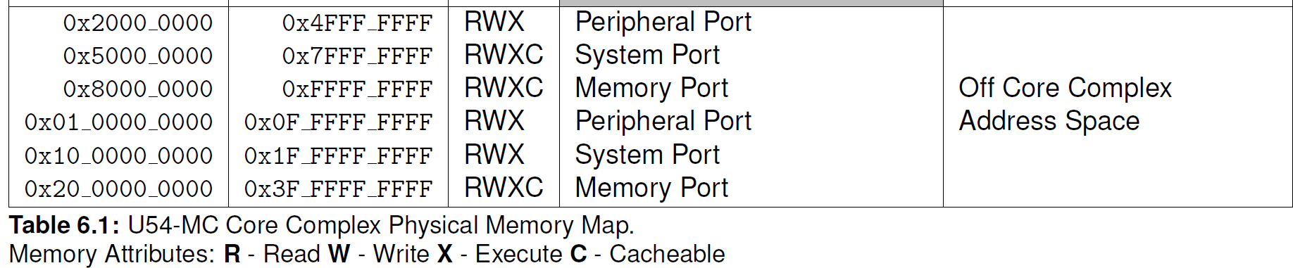
As you can see above, the memory address 0x2000_0000 is NOT RAM. Instead, this will connect us to the peripheral port. It isn’t important to distinguish the peripheral or system ports. However, take a look at our RAM, it’s actually connected at 0x8000_0000 and 0x20_0000_0000. This might look weird, but it’s because the system I’m showing above is a 64-bit system, and NOT a 32-bit system.
Say we wanted to communicate with the peripheral port, with MMIO, we just need a pointer. 0x2000_0000 is called the base address. There are several devices that can be connected here, but let’s just assume for the sake of this example that our device’s control register is connected at 0x2000_0010, and that the register is 2 bytes (a short). To communicate with this register, we just need to do the following.
int main() {
   volatile unsigned short *dev = (unsigned short *)0x20000010;
   *dev = 1 << 2;  // Set bit index 2
   printf("Device gave us %d\n", *dev);
   return 0;
}
It’s not important to know what setting bit index 2 does. I just made that up. We’d actually have to look at the devices technical specification to see what bits in the device’s control register does what. Instead, all I’m showing above is that we can use a pointer to communicate with an MMIO-connected device. These specifications usually provide a table that shows a base address followed by offsets. The base is the memory address where the first register is connected. The offsets are numbers added to the base address to get to particular registers. The able below is an example of a base/offset table:
One thing you might be unfamiliar with is the keyword volatile. This keyword disables the C++ compiler’s optimizer for this pointer. C++ thinks that we as the programmer are the only one that can set and clear bits. However, remember, status bits are being set by the hardware device. C++ won’t know this, and without the volatile keyword, C++ doesn’t expect any register to change without US as the programmer changing it. When we add the volatile keyword, we’re telling C++ that the value at that memory address can change without us doing anything, which is called a side-effect.
We use the volatile keyword since behind the scenes, the devices register can change without us doing anything to change it. Take for example, the case of a keyboard. When I press a key, the device’s internal registers change. We can then poll that change, which means we keep checking the device’s register for any change that might occur, to see what actually occurred.
Sometimes checking a device’s register is not efficient, since checking requires a load operation from the CPU and the memory controller. In many circumstances, the IO device can generate what is known as an interrupt, which is as simple as flowing electrons through a pin directly on the CPU itself. This interrupt then tells the CPU that “something here has changed!”
To recap, PIO requires special assembly instructions to communicate on a dedicated IO bus, whereas MMIO uses simple loads and stores to communicate using the memory controller.
Character Oriented I/O
Character oriented I/O refers to a IO system where we read about one-byte (one character) at a time. I say about because sometimes this can be a bit smaller than one byte or somewhat larger than one byte. However, the point of character I/O is that one of our status registers is used as a receiver which contains data the device wants to communicate with us, and one control register is used as a transmitter which we as the programmer put data in to send over to the device.
Think about the console that we use. This is a character-oriented IO device. Whenever we type something on the keyboard, it goes to the console. One of the status registers tells us that there is data ready. Whenever our program sees this, it can then read the receiver register, which will contain which key was pressed. Whenever the console wants to put text to the screen, the program we use (printf, cout, etc) will write the character into the transmitter control register, which then gets printed to the screen.
Block Oriented I/O
A different style of I/O is known as block-oriented IO. Hard drives and other large data IO systems use block-oriented IO. In this case, we still have control and status registers, but the point of these registers is to set up a central communication channel. Generally, we use a place in RAM as our communication channel. We then use the control register to tell the hardware device what memory address it needs to look into. Whenever we want to communicate, we write our request in that memory location and then press the “GO” button by writing to a specific control register (usually called a notify register). This tells the hardware device that we did something, anything. The hardware device then goes to the pre-configured memory address to see what we actually wrote.
The reason we call this block-oriented I/O is because we transfer blocks. For hard drives, the blocks are usually 512 bytes or even 1024 bytes at a time. This is why we need to use RAM to store this. A register that stores 512 or 1024 bytes would be cumbersome, plus we don’t have a data type that stores 512 or 1024 bytes at a time. So, instead, we use memory as the central communication channel. We only use the status and control registers to tell the hardware device that something happened and to configure what memory address both we and the hardware device are going to use.
Busses
The CPU is busy enough running instructions, so many of the things that take more time are offloaded onto other systems. The following snapshot shows the bus controllers on my personal computer.
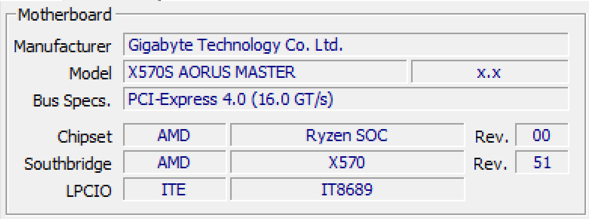
The components are laid out generally as follows.

- Chipset – the chipset is a package to control the memory and input/output devices for the CPU. The CPU commands and is connected to the chipset directly through the front-side bus (FSB).
- South Bridge – some chipsets are further divided into an IO Controller Hub (ICH). This hub talks directly to the chipset, which then can forward the information to the CPU.
- LPCIO – the LPCIO is an offload device that controls the signals to and from the IO devices. LPC stands for “low pin count” and IO stands for “input/output”.
Direct Memory Access (DMA)
The DMA controller is configured by the CPU. The purpose of DMA is to transfer data from a slow I/O device into memory or vice-versa. The CPU can configure the DMA and say, “get this data from this device and put it here in memory.”. The CPU is not involved during the transfer. The DMA does its work and then interrupts the CPU to say, “I’m done!”. The data is directly transferred from the device into RAM or from RAM into the device.
Peripheral Component Interconnect [Express] (PCI/PCIe)
PCI express is the most common way to add expansion devices to modern computers. The PCI bus is rather complicated, so I will not go into the details. Instead, the important part to know is that the PCI/PCIe bus controls all of the devices connected to it.
The PCI bus was invented to make it easier to discover and configure devices attached to a system. In the “olden” days, a physical pin was configured using a jumper. This means that configuration was done when the computer was off, and the device could not be configured when the system was on. A jumper was a small piece of metal coated in plastic to connect two pins.

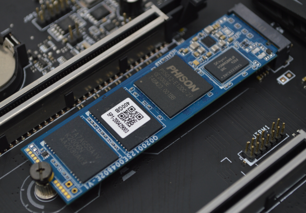
Non-Volatile Memory Express
The non-volatile memory express (NVMe) protocol is a new protocol for solid state drives. Before NVMe, hard drives, even solid state drives, were required to go through the serial-ATA protocol (SATA). However, this protocol was not built for solid state drives as ATA is the old 1970s standard for connecting hard drives–although 90s and before used PATA or parallel-ATA.
The NVMe protocol is ran via devices on the M.2 bus, which is connected directly to the CPU through a high-speed IO bus (HSIO). We will cover HSIO later in this chapter.
Signaling
The actual wires that connect these components need to be connected in a way to make everything we have talked about above possible. Signaling isn’t just for external wires to connect, such as for Ethernet networking, but it is also used on the motherboard. For example, PCI express uses differential signaling on its wires to prevent data corruption. More information about differential signaling is below.
Differential Signaling
Transferring data over a wire is simply send voltage across or not and then wait until the clock on the other side has had a chance to sample it. However, as we know with wires, they can be subjected to interference. This mainly occurs when some other sort of electric device is nearby. Furthermore, there is resistance in a wire. Therefore, the strong voltage sent on one end is not “felt” on the other end.
When it comes to wireless, sending out a signal can lead to other problems. First, there is still interference, especially if the data is being sent at the same frequency. Second, there are security issues. An omni-directional antenna sends data out in all directions without a care in the world who hears it.
The physical limitations of wires has led to a lot of discovery in the best way to transfer data. A technique called differential signaling can be used to cancel out interference provided the wires are close enough to receive the same interference and at the same power.
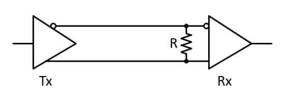
Differential signaling uses two wires to send out the same information. However, the information is inverted. Any interference on the wire should interfere with both wires equally. Since the information is inverted, the difference between them can be subtracted. The subtractor circuit removes most of the interference.

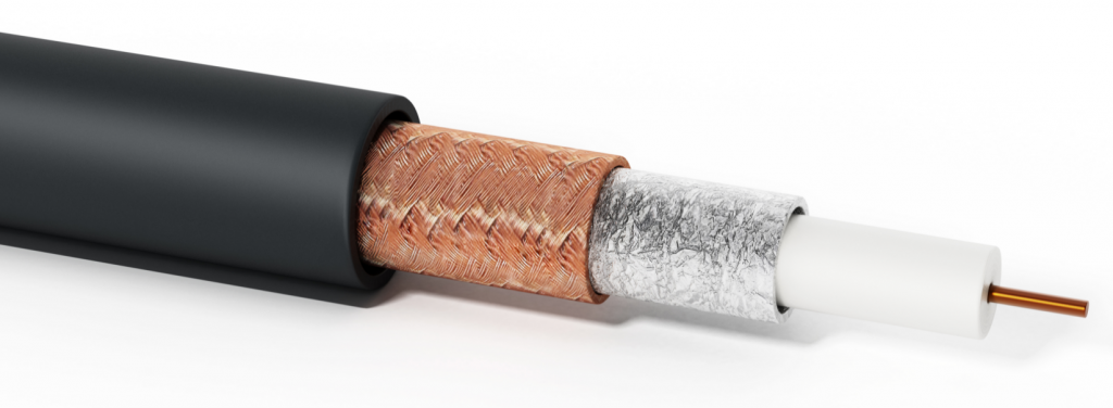
Without differential signaling, shielding would need to be used to remove magnetic interference. This is how coaxial cabling works. There is a braided or foil shield around the conductor which intercepts interference and drives it to ground.
For even longer distances, shielding and differential signaling are used. For very long distances, fiber-optics can be used instead.

High Speed IO Lanes (HSIO)
Some devices transfer a lot of data, such as a graphics processing unit (GPU). The bottlenecks between busses make it so that these types of devices cannot realize their full potential. So, instead, there is a connection method directly to the CPU through high-speed IO lanes (HSIO). When you configure a device, such as a GPU, you will need to see how many lanes it uses to see if it is connected to all of them. Each lane is a differential pair of wires.
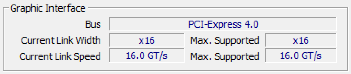
My personal computer has a graphic interface connected to PCIe version 4.0. However, the important part is the current link width. It shows x16, which means that it is connected to 16 lanes. The maximum supported is also 16, so my GPU is using the maximum number of lanes. Each lane is a serial connection, so the more lanes, the more data can be transferred in a given amount of time.
Lanes come at a premium. For example, the Ryzen 9 5950x has 24 PCIe lanes. Currently, the only two types of devices that utilize these lanes are NVMe (Non-volatile Memory Express) hard drives and graphics processing units (GPUs). Since 16 of my lanes are being used for the GPU alone, I only have 8 lanes for the NVMe devices. For computers with multiple GPUs, they are usually negotiated down so that they split the lanes. For example, two GPUs would use 8 lanes each, whereas four GPUs would use 4 lanes each. Therefore, adding two GPUs isn’t necessarily better by two times.

Serial vs Parallel I/O
We used to have PATA (parallel-ATA) that connected our hard drives to a bus. Now, we have SATA (serial-ATA). So, you might think that serial is better than parallel? What’s the difference.
Serial refers to the fact that one follows another. That is, when I want to transmit 8 bits, I send one at a time and toggle a clock each time. This means it takes 8 clock cycles to read 8 bits.
Parallel refers to the fact that more than one bit is signaled simultaneously. If we had 8 wires connecting 8 bits, it would only require 1 clock cycle to read 8 bits.
A serial I/O only needs two wires: the clock and the value, whereas our parallel I/O needed at least 9 wires (8 for the data and 1 for the clock). Not all I/O protocols follow this, but it suits our example.
Serial has been preferred over parallel mainly to reduce the number of inputs and outputs a device needs to have. The Universal Serial Bus (USB) only requires 4 pins: (1) power, (2) transmit, (3) receive, (4) ground. The newer and faster versions have more pins, but you can see with just four pins, we can do a lot of work!
Serial performance is highly dependent on clock speed, whereas parallel performance is highly dependent on the cable. You see, the smaller diameter of wire we have, the more resistance and heat we get over a longer distance. This heat steals away our signal and noise can be injected by alternating current and other signals.