Learning Objectives
- Be able to draw a truth table.
- Be able to put logic gates together to perform a certain function.
- Understand how an OR, AND, and NOT gate work.
- Be able to write a circuit equation from a truth table or diagram.
- Be able to draw a diagram from a circuit equation or truth table.
- Be able to use product-of-sums (POS) and sum-of-products (SOP) forms.
- Understand and be able to apply DeMorgan’s laws.
Depicting a Circuit
There are essentially three ways we can depict a circuit: (1) a truth table, (2) a circuit diagram, and (3) a circuit equation. There are other ways, but these are the ways we will depict circuits in this course. A truth table gives you a big-picture view of a set of inputs and the associated output. It doesn’t show how you get from inputs to output, it just shows what you get. A circuit diagram shows the wires that “flow” electrons from one end to another. This depicts how electrons go from an input put into an output pin. Finally, a circuit equation is much like a truth table, except we can reduce them using Boolean algebra and k-maps (covered later).
Truth Tables
A truth table is a table (go figure??) that shows all of the possible inputs and what output each set of inputs produce. Here’s an example of a & b in C++:
| A | B | \(A\land B\) |
|---|---|---|
| 0 | 0 | 0 |
| 0 | 1 | 0 |
| 1 | 0 | 0 |
| 1 | 1 | 1 |
Each input is 1 bit a piece, so we will have exactly \(2^\text{number of inputs}\) rows. You can see we have 2 inputs above, so we have \(2^2=4\) rows. A truth table’s rows can really be in any order, but typically, to make it easier to read, we start with 0 and increment by one each time we go down a row.
Circuit Diagrams
A circuit diagram uses special iconography to depict circuits. You will recognize the name of many of these icons because we’ve used them in C++. These icons are called Boolean logic gates because a certain condition must be met to give an output.
The “gates” that I will show below are a high-level picture of the gates. Most gates are built using transistors, but we don’t really want to get that low into the weeds. We really only care about putting these gates together to produce a desired output given a certain set of inputs.
The AND Gate
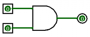
The AND gate requires both inputs (square blocks on the left) to produce an output of 1 (circular block on the right). The AND gate looks like an elongated-D. The following truth table depicts an AND gate.
| A | B | \(A\land B\) |
|---|---|---|
| 0 | 0 | 0 |
| 0 | 1 | 0 |
| 1 | 0 | 0 |
| 1 | 1 | 1 |
To produce an output of 1, both inputs must be 1. There are several ways to depict and AND gate using an equation.
$$Q=AB$$
$$Q=A\bullet B$$
$$Q=A\times B$$
$$Q=A\land B$$
In a circuit equation, AND is equivalent to multiplication. You’ll see why we can treat AND as a multiplication operation when we start reducing circuits using Boolean algebra.
Don’t confuse \(\land\) with the C++ operator ^ (xor)!! During this lecture, we’re not talking C++.
The OR Gate
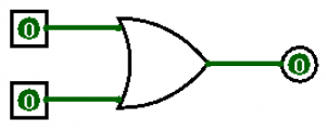
Just like the C++’s logical OR, we have an OR gate for circuit diagrams:
The following truth table depicts an OR gate and its associated outputs.
| A | B | \(A\lor B\) |
|---|---|---|
| 0 | 0 | 0 |
| 0 | 1 | 1 |
| 1 | 0 | 1 |
| 1 | 1 | 1 |
The OR gate is equivalent to the addition operation in a circuit equation:
$$Q=A+B$$
$$Q=A\lor B$$
The INVERTER (NOT)
We can flip 1s to 0s and 0s to 1s by using an inverter, depicted below.
The triangle portion of the inverter is called a buffer. A buffer just holds a value. The actual inverter is the little circle on the tip of the triangle. You will see these circles again. These are called inverter bubbles. We can put inverter bubbles on any input or output of any gate. Anytime we see this little bubble, we invert the input to the opposite value (1 goes to 0 and 0 goes to 1.
| A | \(\neg A\) |
|---|---|
| 0 | 1 |
| 1 | 0 |
The NOT gate only takes ONE input and inverts it. There are several ways to depict a NOT gate in a circuit equation. Here are some examples:
$$Q=A’$$
$$Q=\neg A$$
$$Q=\bar A$$
The XOR gate
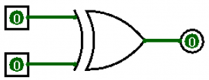
The exclusive OR (xor) is not a real circuit, but it helps us minimize our circuit diagrams to make them more readable. In fact, the XOR gate is made up of AND and OR gates, which I will show later. The XOR gate looks like the following.
The exclusive OR gate looks much like an OR gate, except it has TWO curved lines on the input side. The XOR gate works just like the XOR operator in C++ and has the following truth table.
| A | B | \(A\oplus B\) |
|---|---|---|
| 0 | 0 | 0 |
| 0 | 1 | 1 |
| 1 | 0 | 1 |
| 1 | 1 | 0 |
We use the “circled plus” to depict an XOR in a circuit equation:
$$Q=A\oplus B$$
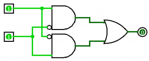
I said before that an XOR can be implemented by using just AND and OR gates. I won’t leave you hanging, below is an implementation of XOR using AND and OR gates only.
Notice we have two AND gates and one OR gate. Also notice the small little circles on one of each AND gates’ inputs. Recall that this is the inverter bubble. Whenever that bubble sees an input of 0, it produces an output of 1. Whenever that bubble sees an input of 1, it produces an output of 0. The circuit equation for the diagram above looks as follows.
$$Q=AB’+A’B=A\oplus B$$
Notice the pattern here. One non-inverted input AND’ed with an inverted input then OR’ed with the exact opposite inputs. This “staggered” equation identifies an XOR (exclusive or) operation.
The NOR, NAND, and XNOR Gates
We call an OR gate with an inverted output a NOR gate (not-OR). We call an AND gate with an inverted output a NAND gate. Finally, we call an XOR gate with an inverted output a XNOR gate. We only change the name of the gate when the output (notice all the bold and italics I used) is inverted. When the inputs are the only thing inverted, we still call it an OR, AND, or XOR gate.
Making Equations
Given a truth table, we can make a circuit equation using one of two ways: (1) sum-of-products (SOP) and (2) product-of-sums (POS). Both use only AND and OR gates, but the flow order is flipped. For SOP, AND gates feed into OR gates (we take the sum (OR) of the products (AND)). For POS, OR gates feed into AND gates (we take the product (AND) of the sums (OR)).
Sum-of-Products (SOP)
For sum-of-products, we look at a truth table and ONLY consider rows whose output is 1. Any other row whose output is 0 is ignored. We combine columns using AND gates and we combine all rows (whose output is 1) using OR gates. Finally, we invert any input that is 0 and leave any input that is 1 alone. Many times, you will see the output as the variable Q, which I used below.
Here’s a 3-input truth table and the associated equation using SOP.
| A | B | C | Q (output) |
|---|---|---|---|
| 0 | 0 | 0 | 0 |
| 0 | 0 | 1 | 1 |
| 0 | 1 | 0 | 1 |
| 0 | 1 | 1 | 0 |
| 1 | 0 | 0 | 0 |
| 1 | 0 | 1 | 0 |
| 1 | 1 | 0 | 0 |
| 1 | 1 | 1 | 1 |
For the SOP form, recall that we look only where the output is 1. We can see that we have 3 different rows whose output is 1 (001, 010, and 111). Recall also that when we move to another column, we combine them using AND gates. We also need to invert any input that is 0. So, 001 needs to invert the input A and the input B while leaving C alone. So, this one row would have a circuit equation of:
$$Q=A’B’C$$
Then, we look at 010 and 111. 010 needs the inputs A and C inverted (since they are 0) and 111 needs NOTHING inverted. Recall that we combine each set of inputs using OR gates, which is the addition operation.
$$Q=A’B’C+A’BC’+ABC$$
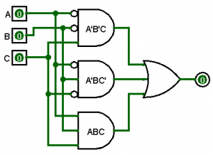
Our completed circuit equation is above. We can double check our work by plugging in 001 into the equation above. Notice that produces an output of 1. Then plug in 010, which again, produces 1. Then plug in 111. That produces an output of 1 too! Everything else produces an output of 0, so it mimics the truth table nicely! To draw the circuit diagram, we can use 3-input AND gates and use inverter bubbles. Recall that in SOP, AND gates feed into OR gates. We need a 3-input OR gate since there are three rows.
You can see the inverter bubbles on the A and B pins for the first AND gate to depict \(Q=A’B’C\), then inverter bubbles on the A and C pins for the second AND gate to depict \(Q=A’BC’\). Finally, we have no inverter bubbles on the third AND gate to depict \(Q=ABC\). Notice again that the AND gates are perform FIRST, followed by the OR gate. This is why we call this form the sum-of-products or SOP.
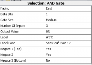
In Logisim, we can change the number of inputs, the label, and which inputs are inverted using the toolbox on the left.
See the “Negate”? If we set this to Yes, an inverter bubble will be added. Make sure you do this BEFORE you connect the wires!
Product-of-Sums (POS)
The other form we can use is the product-of-sums or POS form. Essentially, in this form, we do exactly the opposite of SOP. Instead of looking for an output of 1, we look for an output of 0. Instead of inverting inputs of 0, we invert inputs of 1. Instead of combining columns using an AND gate, we combine columns using an OR gate. Instead of combining rows using an OR gate, we combine rows using an AND gate. Let’s see an example of POS.
| A | B | C | Q |
|---|---|---|---|
| 0 | 0 | 0 | 0 |
| 0 | 0 | 1 | 1 |
| 0 | 1 | 0 | 1 |
| 0 | 1 | 1 | 0 |
| 1 | 0 | 0 | 1 |
| 1 | 0 | 1 | 1 |
| 1 | 1 | 0 | 1 |
| 1 | 1 | 1 | 0 |
We can see that there are three rows where the output is 0. Remember, we invert columns of 1 and combine them using OR gates:
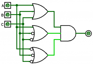
$$Q=(A+B+C)(A+B’+C’)(A’+B’+C’)$$
Here we go! I combined the columns using OR gates. Since these are in parentheses, those operations are performed first. Finally, each of these groups (terms) are multiplied together, this is done last. This is why we call this taking the product of the sums.
We generally choose one form over the other based on which one has fewer terms. If there are fewer outputs that are 0, choose POS. If there are fewer outputs that are 1, choose SOP. Or, during an exam, I might tell you which one to use.
DeMorgan’s Law
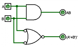
Both forms are equivalent in producing the output of the truth table. This is done using DeMorgan’s Law. This law is fairly simple, we change all ANDs to ORs and all ORs to ANDs. Then, we invert was was previously NOT inverted. So, all inverted inputs become not-inverted (for lack of a better term), and all not-inverted inputs become inverted. When inverting, do NOT forget about the output! We can see this by demonstrating equivalent circuit diagrams.
$$Q=AB=(A’+B’)’$$
In the circuit diagram above, we can see that \(Q=AB\) and \(Q=(A’+B’)’\) produce equivalent results.
Formally, DeMorgan’s laws are depicted by the following transformations.
$$\neg(A\lor B)\iff (\neg A)\land (\neg B)$$
$$\neg(A\land B)\iff (\neg A)\lor (\neg B)$$
